
Characterizing functional solid materials:
the challenge of non-standard geometry and morphology
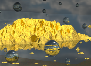
Artistic depiction of a carbon-nitride photocatalyst, synthesized on a silicon wafer: how to gain insight into its opto-electronic properties? © C. Merschjann
Novel functional materials are at the heart of new developments in technology. Some important fields include:
- renewable energies
- micro- and nanoelectronics
- medical technology
- composite-material engineering
In all cases, one will be interested in quantifying the properties of the materials, so as to assess their applicability for the intended – or unforeseen – uses. In our case, we are mostly concerned with opto-electronic properties, such as conductivity, the absorption or refraction of light, or – in more general terms – the dielectric function of the material. And since devices are used in non-equilibrium conditions, e.g., a solar cell under light exposure or a working LED, we want to explore the dynamics of these properties using time-resolved techniques.
However, most novel solid materials do not initially come as textbook-standard specimens like single crystals, or thin films, but usually as powders. And moreover, many state-of-the-art technologies do not use these materials in standard geometries: photocatalysts should have maximal surface area, and are therefore applied as sponges; medical applications use nanoparticles as markers or drug-release agents; electronic circuits have a complicated geometry, etc.
In addition, the materials themselves are applied as hybrids, comprising several different pure compounds in one microscopic volume: bi-phase particles for photocatalytic water splitting and bulk-heterojunction solar cells are examples for this.
Under these circumstances, many well-established electrical characterization methods, like four-point-probe, Hall- and Seebeck-conductivity techniques, tend to be not applicable or to yield misleading results, disregarding the microscopic structure of the samples under investigation.
We have therefore apllied steady-state and especially transient optical spectroscopy to gain insight into the static and dynamic opto-electronic properties of novel solid materials.
Here, we concentrate currently on materials intended for photocatalytic applications – most prominently solar water splitting – but also for (organic) electronics in general. The most prominent material class in our focus are polymeric (often somewhat misleadingly termed “graphitic”) carbon nitrides (“g-C3N4“), which have been investigated quite heavily in recent years for their potential application in metal-free catalytic water splitting, and also in electronics, photovoltaics, solid-state lighting etc.
See here for a recent Review of functional carbon nitrides.
Getting insight into the dynamics via transient optical spectroscopy
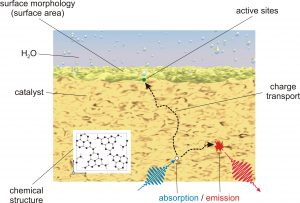
Simplistic sketch of the processes in a heterogeneous photocatalyst: from excitation to catalytic reaction. © C. Merschjann
When exposed to light with photon energy larger than its electronic bandgap, electrons in a material are promoted to excited states. For semiconductors, these initial excitations typically assume the form of excitons, free carriers, or self-trapped carriers (polarons). This leads to a change in the complex refractive index of the material, which is most prominently visible as a change in absorption coefficient, and is proportional to the number density of excited carriers.
Transient absorption (TA) spectroscopy records these absorption changes as a function of time, thus giving a direct measure of the respective excited states.
A complementary tool is transient photoluminescence (TRPL), which records the emission of photons upon recombination of excited carriers. While typically this is the easier experimental method, compared to TA, it measures the “death” of an excitation, rather than its “life”. Therefore, TRPL signals are in general not directly proportional to the concentration of excited states. In fact, such a proportionality is given only in the case of exponential decays, which are the rule for molecules, but the exception for solids.
In order to be able to record TA data from powder samples, we have developed a dedicated TA setup that can be operated both in conventional transmission, and in diffuse reflection geometry.
Combining both transient spectroscopy methods, we are able to investigate light-induced excited states from tens of femtoseconds to the millisecond range. Thus, we monitor the early excitation processes, spatial transport of charges, and their recombination over many decades in time.
Dimensionality matters…
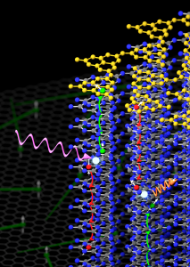
Depiction of light-induced charge transport in polymeric carbon nitride. Confinement of the carriers in 1-dimensional channels leads to characteristic decay curves. © C. Merschjann
It has been shown that the fate of a photoexcited charge carrier depends crucially on the dimensionality of its environment, i.e., whether it can move in 3-dimensional space, or is confined in lower dimensions. These conditions affect not only the lifetime of the carriers, but lead to very characteristic decay shapes in both TA and TRPL traces. Thus, it is possible to deduce the dimensionality of the system from the decay curves.
We found that the relaxation kinetics of excited carriers in carbon-nitride polymers are quite peculiar, leading us to conclude that we are facing a material class where charge transport is confined to low dimensions (most likely one-dimensional) within a three-dimensional bulk solid. Read more in our article in Advanced Materials.
Further experimental observations are currently being analyzed. Since the underlying transport scenarios are quite complex, we use random-walk models to describe the dynamics, both via rate equations and numerical simulations (Monte-Carlo methods). The respective elementary transport steps are being elucidated with the help of dedicated theory partners.
Detailed descriptions of experimental setups, theories and simulational methods will be given here in the near future…